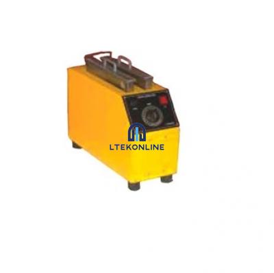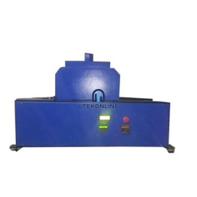
Tenders Description & Specification for PCB Lab Kit Exposer Developing Etching Machine
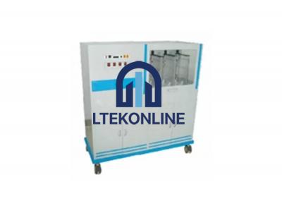
PCB Lab Kit Exposer Developing Etching Machine
Vacuum dual exposure 2. Imaging function 3. Circuit board corrosion function 4. Circuit board via hole function
Feature
It uses environment protection transparent material, students can see the whole process for go through holes.
Drawer type exposure function, it has vacuum sucker function, time control function, image function is made of transparent material.
Technical parameter
Circuit board plate making precision: 4-6mil, 0.1-0.15mm
Max image function dimension: 300×200mm(Transparent corrosion slot 1 set )
Max corrosion dimension: 300×200mm(Transparent corrosion slot 2 sets )
Max holes dimension: 300×200mm(Transparent corrosion slot 2 set )
Temperature controller: 45-65, and it is adjustable
Minimum through hole precision:φ0.3mm
Pump work pressure: 1.2KW
Work power: 220V, 50Hz
Dimension: 1700×1200×400mm
Ltekonline are the manufacturers of PCB Lab Kit Exposer Developing Etching Machine used to demonstrate engineering principles in Engineering Colleges, Engineering Schools and PCB Lab Equipment for Engineering Teaching Lab in Universities
Categories: PCB Lab Equipment